Application of Aberration-corrected electron
microscopy in resolving atomic and electronic structures of interfaces
Interfaces are the important link between different materials as well as
breeding grounds for new phases and novel phenomena. They have long being the object of
fascination, but remain relatively inaccessible, for example, comparing to
surfaces of solids. With the
development of atom-resolving electron microscopy such as that available in York
JEOL Nanocentre and the
application of atomically resolved EELS spectroscopic technique, we are
uncovering the complexity of interfaces in materials and devices both large and
small.
Interfaces in Boron-rich nanowires
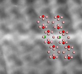
Monolayer segregation of Ba
atoms seen in Boron suboxide nanowires
using High angle annular dark field Scanning Transmission Electron Microscope
(HADDF-STEM)
Interface in ferrite materials
X ZHANG, WG WANG, LN ZHANG, JJ QI AND J YUAN
Correlation
of bonding of grain boundary and fracture mode with local electronic structure
in steels by electron energy loss spectroscopy
Appl. Phys. Letts., 90, 171905 (2007).
XZ ZHANG, LN ZHANG, Y MA AND J YUAN
Electronic
Structure Characterization of Bonding of Grain Boundaries and Fracture Mode of
Steels
Acta Metallurgica Sinica, 41(6), 617-621 (2005).