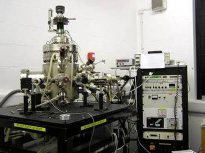
- UHV growth
chambers with three e-beam sources, two sputtering sources and a
sample transfer chamber.
- In-situ
Structural analysis using RHEED
- In-situ
Magnetic and magneto-elastic properties measurements
- Advanced
photolithography (a mask aligner up to 3 inch wafers, a photoresist
spinner, and a wet chemical workstation)
- Advanced
e-beam lithography (NanoCenter)
- Focused Ion
beam for lithography (NanoCenter)
- Atomic force
microscopy/magnetic force microscopy/scanning tunneling microscopy (NanoCenter)
- Plasma Enhanced
Chemical Vapour Deposition (PECVD)
- A plasma
reactive ion etcher (RIE)
- Thermal
Oxidation
- Scanning
Electron Microscope.
- Ex-situ and
in-situ MOKE for magnetic characterisation
-
Magneto-resistance, I-V characterisation and spin dependant
transport measurements
- A well
equipped class 100 clean room for device fabrications and testing
- Facilities
in central laboratory of research council, Daresbury Synchrotron
Radiation Laboratory and Diamond Laboratory
|
 |