Last updated: 27/12/2018
Introduction to Spintronics
The second major progress is the observation of tunneling magnetoresistance (TMR) at room temperature (RT) in 1995, derived from spin-dependent electron tunneling through an oxide barrier, which has been replaced with the non-magnetic layer in the GMR systems. The TMR offers a much larger MR ratio between the parallel and anti-parallel resistances, improving a signal to noise ratio for a higher areal density in a HDD.
In concurrent with these magnetoelectronic discoveries, materials science has also contributed to the rapid development of spintronics. On account of recent advance in vacuum technology, these films, not only ferromagnetic films but also non-magnet including oxides, are able to be grown epitaxially, which has further improved the magnetic properties, such as the TMR ratios.
Nano-fabrication is another key to broaden the spintronic device applications. Reduction in the junction area restricts the spin transport path into pseudo-1-dimensional pillar or wire, and also eliminates unfavorable defects at the junction interfaces, such as pinholes. Further reduction in size, even with precise atomic structure control, leads to creation of new spintronic materials (half-metallic ferromagnets), which confers unique magnetic characteristics, 100% spin polarisation and large magnetic anisotropy for instance.
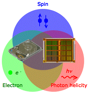
 Combination of the above nanoelectronics and materials science affords a platform for spintronics, where spins, electrons and photons interact with each other, realising spin-polarised electron transport, very large spin polarisation and photo-induced spin dynamics, etc. The integration of these three fundamental particles will promote future spintronic applications, a polarisation-tunable spin source, a spin transistor, spin diode and so on, each of which is anticipated to incorporate many accessible functionalities in conventional electronics.
For further reading Back to the Top Spintronics Research >


