Last updated: 11/09/2019
Growth Facilities
UHV MBE/sputter
HiTUS
Nanofabrication
e-beam lithography
Photolithography
FIB
Cleanroom
Characterisation
Probe station
XRD
GHz pulse measurement
Dilution refrigerator
VSM
AGFM
MR prober
Probe station
Annealing furnace
MOKE
HRTEM/STEM
TEM
SEM
SPM
Sample preparation
Particle analyser
E-Beam Lithography
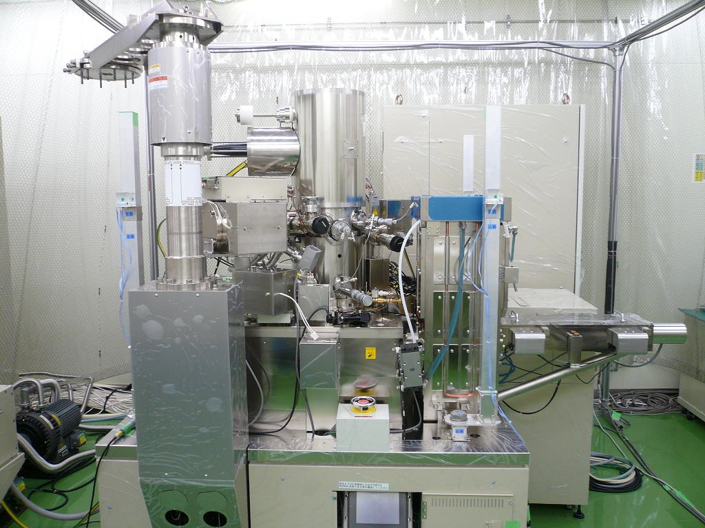
JEOL JBX-6300FS

This system is under construction by JEOL and is planned to be installed in the University of Leeds by the end of June 2011. Our group has 25% of the quota with a dedicated experimental officer to be appointed. This system satisfies the following capabilities:
- Acceleration voltage: 25, 50 & 100 kV
- Electon gun: ZrO/W Schottky
- Electron-beam: < 2 nm in diameter
- Wafer handling: 10 wafer loader (5 mm square ~ 4" wafer)
- Overlay accuracy: < ± 20 nm
- Stitching accuracy: < ± 20 nm
- Minimum feature: < 10 nm

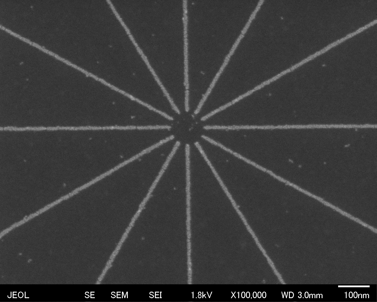
Example of a rosette cinsisting of 10 nm wide metallic wire.